Training report at INSP
Charlie Leprince
Yohann Roiron
Damien Toussaint
Training supervisor: Stéphane Pons
http://olympiades.pothier11.free.fr/ |
Acknowledgments
We want to thank the INSP members for the warm welcome: the INSP director B. Perrin, our training supervisor S. Pons, and the team of tunneling microscopy and spectroscopy for its explanations: D. Roditchev, C. Brun, C. Carbillet, V. Cerchez, T. Cren, F. Debontridder, K. Khazen, Y. Noat, L. Serrier-Garcia.
We also thank the headmaster of the Lycée Pothier, B. Plasse, for his helping and his support, and MC. Baurrier, for her encouragements.
Introduction
The INSP (Institut des Nanosciences de Paris/Nanosciences Institute of Paris) is a laboratory where nanomaterials are studied. The researchers analyze samples and their properties in order to understand the behavior of material at the nanometric scale. Indeed, at this scale, phenomena are not the same as at higher (i.e. macroscopic) scales.
The institute is in the UPMC (Université Pierre et Marie Curie/Pierre and Marie Curie University), and this is where we made our training.
The aim of our project "Diving into the invisible" was to see the matter. At INSP, the Scanning Tunneling Microscope (STM) is used to study the surface properties of samples. We wanted to understand how to prepare the samples in order to analyze materials with STM. The team we worked with focus mainly on the superconducting properties of samples (http://www.insp.jussieu.fr/-Dispositifs-quantiques-controles-.html).
Superconductors
A conductor material conducts current (its resistivity is very low, like copper: 1,72 .10-8 Ω.m), whereas nonconductor material doesn't (its resistivity is very high, like polystyrene: 1,00.1020 Ω.m).
Superconducting materials have no resistivity, if they are enough cooled. There are two kinds of superconductors: some (most of non-magnetic and non-noble metals) are superconductor at a very low temperature, near 4K. This class of materials is well understood. Other "non-conventional" superconductors, with higher critical temperature, near 90K, also exist. The understanding of these materials is a scientific challenge for 25 years now.
The superconductors have many advantages and applications, like the transport of electricity, production of high magnetic fields (e.g. for Magnetic resonance imaging) and quantum informatics, thanks to the low resistivity and the global behaviour of electrons.
The aim of the researchers is to understand and theorize the macroscopic and the microscopic behaviour of such materials: the researchers at INSP mainly focus on the interplay of superconductivity and low dimensionality (which refers to the dimensions and their effects).
Macroscopic observation

Fig. 1 - The superconductor pellet
During our stage at INSP, we were introduced to the superconducting behaviour of materials belonging to the second family of superconductor, which can be cooled thanks to liquid nitrogen (less expensive than liquid helium, which is used to cool the first family of superconductor). The superconductor we saw was a pellet of yttrium-barium-copper-oxygen (YBaCuO).
 It's a ceramics, which has been compressed in order to shape it (fig. 1).
The pellet does not interact with magnets at ambient temperature.
Its resistivity is very important, that's why it's a bad conductor (or insulator) at such temperature.

Fig. 2 – Levitation of a magnet above a cold superconductor
When the pellet is cooled at 77K (at liquid nitrogen temperature), lower than the critical temperature, it becomes superconductor: its resistivity is null. But if the pellet is warmed, the material becomes nonconductor again. So, there is a reversible phase transition from bad conductor to superconductor.
A quantic phenomenon is responsible of the superconductivity: below the transition temperature, the electrons behave as a wave. They also have a global behavior in the sample and move with the same phase.
We can make a superconductor levitate above a rail of magnets (fig. 3): there are in fact no frictional forces. If we cool the superconductor above the rail, we can observe this material levitate. If we cool the same material somewhere else than above the rail, it would not levitate as good.
In the two cases, the levitation lasts until the superconductor becomes warm back and can be observed no matter the direction and the orientation of the rail is.


Fig.3 – Levitation of a cooled superconductor into polystyrene above a magnetic rail
Microscopic explanations
The levitation of a superconductor material above a rail of magnets is due to an interaction of repulsion between this material and the magnetic field of the magnets. Indeed, the electrons of the superconductor will try to repulse the magnetic field of the magnets by creating their own opposite magnetic field.
When a superconductor, which has not been cooled above the magnets, is placed above the rail, the magnetic field of the magnets changes the properties of the material (the electrons reorganize themselves) and the field lines stay outside the material and are repulsed, deviated by it: the position is not stable. That's why the superconductor doesn't levitate well. This is called the Meissner effect.
When a superconductor is forced to be just above the rail, the magnetic field is so strong that the superconductor cannot repulse it. Field lines pass through the material and vortexes are created by a collective rotation of the electrons (fig. 4). The magnetic field is trapped in the vortexes and thus, the position is stable; that's why the material levitates well.

Fig. 4 – Vortexes in a superconductor material
Thus, the presence of strong field lines when the material is cooled will enable it to levitate well.
Moreover, the magnetic environment is conserved by the superconductor: there is a balance because changing this stable state costs energy (e.g. in order to introduce a new vortex in the system).
Besides, we can observe that a magnet can have different behaviors with different metals. For instance, it slips well on aluminum whereas it slips slowly on copper. Indeed, the copper has a low resistivity: vortexes are almost created in the material but the resistivity prohibits a perpetual rotation of the electrons. This phenomenon is called Eddy (or Foucault) current.
Instrumentation
STM
The scanning tunneling microscope (STM) is a microscope using a current of quantum origin (the tunnel current) in order to image the topology of the sample surface. Atoms can so be seen thanks to an ultimate resolution of the order of 10-11 meters.
We worked with an apparatus which is constituted by two vacuum chambers: the preparation chamber and the STM chamber. They are separated by a valve (fig 5).


The preparation chamber enables us to prepare the sample in vacuum in order to have a clean surface. In this chamber, we can heat the sample, clean it and realize a "quality control" of the vacuum with a mass spectrometer, analyze the atomic ordering and the symmetry of the sample by Low Energy Electrons Diffraction (LEED). Below the STM chamber, there is a cryostat. It enables us to cool the sample, to reach its critical temperature of superconductivity. In the cryostat there is also a superconducting coil, which is used to create a huge magnetic field.
A load lock chamber is linked to the preparation chamber in order to introduce new sample in the vacuum chamber.
Vacuum
A few days before we came at INSP, the STM chamber had been opened for maintenance: the tip holder of the microscope was blocked. The researchers put it to the atmospheric pressure and repaired it. Then, they had to prepare it for other experiments.
At the atmospheric pressure, there are too many contaminants which could absorb on the surface. For example, if we would study the surface of a sample exposed to the atmosphere, we would just see the atmospheric molecules: indeed, just one second is necessary to recover the sample of contaminants, at 1.0 10-6 mbar. That is why the researchers need a good vacuum, in order to have enough time to analyze the sample. It is called ultra-high vacuum (UHV), whose pressure is around 5.0 10-11 mbar.

Fig. 6 – Turbo-molecular pump
In order to have the UHV, we need several pumps, 6 in all the apparatus. In order to compensate the outgassing of the metallic chamber (mainly hydrogen), they work continuously. The first one creates a first vacuum of 10-2 mbar, in the primary circuit.
Then, there are three pumps, one per chamber and one in the load lock chamber. These turbo molecular pumps are constituted of several blades stages with increasingly large angle. They push the molecules in one direction thanks to a high speed of 70 000 revolutions per minute. These pumps are enough reaching an ultra-high vacuum.
To facilitate and accelerate the UHV establishment, a bakeout is done. All the apparatus were heated to 150° C (423° K) for 3 days. The aim of the bakeout is to sublimate the gas, which deposited on the inner surface during the opening of the vacuum chambers. It enables researchers to get rid of water which is very difficult to pump too. During this operation, the pressure increases quickly, then decreases and finally stabilizes around 10-8 mbar. But during the cooling, the pressure decreases to ~10-11 mb, as the temperature decreases.
Thus, thanks to the bakeout, we obtain the ultra-high vacuum.
Additionally, we use two ionic pumps, which ionize gas. Moreover, thanks to a very high voltage, conjugated to a high magnetic field, the ionized is accelerated gas to a titanium electrode, where a chemical reaction will trap it. This system is very efficient for pumping in the 10-11 mb range and do not produce vibrating noise whereas turbo-molecular pumps do. These pumps are used when performing STM experiments whereas turbo-molecular pumps are turned off because vibrations forbid having a good resolution.
Low temperature
The STM is connected to a cryostat which cools a superconducting coil, to produce a magnetic field.
In order to study the superconducting sample, the STM has to be cooled too. Thus, the microscope is placed on a piece of cooper, which leads the cooling from the cryostat.
The cryostat is like a thermos, and can contain 100 L of liquid helium (fig 7). It must be filled in again each 4 days.
The very low temperature of 300mK can obtained with the STM at INSP.
Fig. 7 – The helium Dewar
Mass spectrometer

Fig. 8 – The mass spectrometer
The mass spectrometer (fig. 8) is an apparatus which enables the experimentalists to control the quality of the vacuum, i.e. to know the nature and the concentration of the contaminants.
The mass spectrometer ionizes molecules. Leaving the ionize chamber, they are then accelerated by a difference of potential of voltage U between two grids. Then they are subjected to a constant magnetic field. The ions have so circular trajectories, depending on their mass. By knowing the radius, we could know the mass of the molecule: that's how we can find the nature of the contaminants. (fig 9).

Fig. 9 – The mass spectrometer principle
In order to detect all the contaminants, they change the voltage U, so the acceleration of the ions is modified, as the trajectory. In fact, the deviation (depending on the mass) stays the same, but, as the ions are more accelerated, they will be deviated later. Thus, by modifying the voltage, all the contaminants will be detected by the detector. It enables the researchers to know the quantity of each contaminant in the vacuum, by measuring the current generated by the ions.
A molecule can be charged twice (or more), so it is more accelerated and is detected like a molecule with a half of its mass.


For instance, on the mass spectrogram, we can see peak at 2 u, which shows that there is dihydrogen in the chamber, 18 u, corresponding to water, and at 32 u, which represents the dioxygen.
Thus we can know the vacuum quality.
The Low Energy Electron Diffraction

Fig. 11 – The LEED principle
Before the STM measurements, we can verify if the atoms are well organized thanks to the LEED (low energy electron diffraction) and know the periodicity of their arrangement.
Electrons are emitted with a filament. The electrons, of the same energy, move to the surface. They are reflected at angles corresponding to the surface order (fig 11).
The interaction between the emitted electrons and the electronic cloud of the atoms is very important: so the incoming electrons are strongly diffracted by the first layer of atoms. That's why it allows the experimentalist to study the surface crystallography. Because the electrons of atoms are distributed in orbitals, the chemicals bonds have particular direction to order. So a crystal shows perfectly ordered lattice of atoms with a particular symmetry.
In a crystal, the distance between two atoms is near 3.10-10 m.
Principle of a STM
The envelope of all the electrons cloud along molecular bond in the crystal has a profile. We can see this envelope with to the STM.
The STM is constituted by a metallic tip above the sample which scans the surface. A voltage bias is applied to the tip with respect to the surface.

Fig. 12 – The tip and the sample
When the distance between the tip and the surface is of the order of half a nanometer, quantum mechanics enables a current to run, even if the vacuum between the tip and the surface is insulating. The electrons behave like a wave whose wavelength has the same order of magnitude than the distance between the sample and the tip. Part of the wave is transmitted through the vacuum to the surface. The intensity decreases exponentially, depending on the tip-surface distance (fig 13). This current is called tunneling current.
The detected current is around 1 nA.
Because we measure a current, STM cannot study insulators.

The intensity of the tunneling current is proportional to the exponential of the distance:
I where k is a constant depending on the voltage and the electronic properties of the material.
Moreover, since the tunnel current depends on the resistivity of the surface, the STM is also sensitive to the electronic properties of the materials. It is a perfect tool for the study the superconductor.
Instead of measuring the intensity which changes a lot, when scanning above the surface, the z axe is constantly corrected to keep fixed the tunneling current. The tip is moved up and down in order to keep the same current intensity.
Fig. 14 – The piezoelectric material

The tip is fixed to a piezoelectric tube (fig 14). The tip can be moved thanks to the piezoelectric materials, whose size depends on the voltage. When operating, the intensity of the tunneling current stays the same (there is a set point for the current). In order to keep the current constant the size of the piezoelectric material is changed.
Thanks to the piezoelectric materials, the tip can be moved very precisely (precision better than 0,1.10-10 m).
So we can measure the distance between the tip and the atoms in order to find the topography of the surface: we can "see" the atoms and the monoatomic steps.
Results
Preparation of an experiment
A silicon sample
During our training, a silicon sample had to be prepared. The silicon is a semi-conductor, which means that it doesn't conduct current very well. If it is cooled, its resistivity increases.
The silicon sample was used because the researchers will deposit nanostructures of lead on it. Lead is superconductor at around 8K, that's why this kind of samples is studied. The effects of dimensionality on superconductivity are analyzed. In theory, if the sample is too small, there is no superconductivity, but there are particular phenomena. At INSP, the limits of the size which enable these phenomena to appear are studied.

The sample has to be cut in order to be introduced in the STM between two lamellae.

The silicon has a hexagonal symmetry (fig 16). It is a (111) silicon. The silicon atoms order like a cube (diamond structure). This cube is cleaved at the (111) plane: a particular surface structure is obtained.

It was outgassed in order to evacuate the oxide layer: the silicon sample was « flashed », which means that it was heated briefly at 1200°C in order to evacuate contaminants. His color changes, because the wavelength of the emitted light depends on the temperature (Fig 18).

Temperature of the sample can be measured thanks to a pyrometer. It is sensible at temperatures between 300°C and 1300°C, corresponding to an infrared light. It measures the emitted energy by the sample and deduces the temperature.
After the heating, it is cooled slowly: the atoms of silicon have enough time to reorganize differently. There is still a hexagonal symmetry, with a new order, called 7x7 reconstruction.
LEED measurements
We check if the atoms are well reorganized thanks to the LEED. We obtain this diffraction picture:

We can see a hexagonal periodic structure. There are also extraspots which correspond to the reorganization of the surface atoms. Indeed, the atoms on the surface of silicon spontaneously reorganize in a structure which is seven times bigger than the crystal lattice (the distance between the spots on the diffraction image is inversely proportional to the distance in the sample). It's called the 7x7 reconstruction of silicon.
Lead sublimation
Then, lead must be deposited on the surface of silicon in order to make "lead islands": we first evaporate it. Researchers want to deposit only a few layers of atoms on the sample. The evaporation must be precise and is not necessarily quick.
The material to evaporate is heated in vacuum and the sample is set in front of it. An evaporator by electrons bombardment is used. Lead is put in a crucible. A filament heated (with an 800 V voltage) emits electrons which head for the crucible (fig 20). The shocks between the electrons and lead create warming: the temperatures increases at 400°C. Lead sublimes and the atoms head for the surface. The atoms order and make a first lead atomic layer on the silicon surface.

Fig. 20 – The lead sublimation principle
Unfortunately, we didn't have time to realize measures of samples with lead during our training. Measures were made on a silicon sample.
Preparation of the tip
The composition of the tips depends on the sample to study. For silicon samples, tungsten points are used. The threads are sharpened by electrochemical erosion. But the tip must be flashed too in order to eliminate the native insulated oxide. Indeed, the tip must be very sharp: there should be only one atom at the top of the tip (fig 21).

Fig. 21 – The example of tungsten tip with an oxide layer

Fig. 22 – A tip on its bracket
In the preparation chamber, the tip touches lamellae, and we run a current between the tip holder and the lamellae, so the tip is heated, but we can't measure its temperature.

STM measurements
On the STM picture, we can see the ordered atoms. There is the 7x7 silicon hexagonal symmetry. Each point corresponds to an atom. Thanks to the measures of the distance z between the tip and the surface, the topology of the sample is imaged.
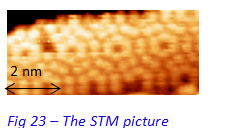
The sample was not so clean (it was an "old" sample which knew many outgassings and flashes) that's why it was hard to find the 7x7 reorganization of atoms thanks to the STM. A long part of the sample seemed not organized.
However, even if the organized surface was very small (near 3 nanometers), and even if the quality of the image is not very good, we succeeded to see the atoms!
Conclusion
Our training enabled us to discover many techniques belonging to many parts of physic (superconductivity, quantum mechanics, and preparation of samples).
We also lived the usual life of researchers: the experiments do not always work, there are sometimes technic problems to solve, but it is another way to learn.
Moreover, we saw another microscope which studies the surface properties: the Atomic Force Microscope (AFM). Contrarily to the STM, it can analyze all the materials. It is constituted by a tip, and the forces between the tip and the surface are studied. A diapason is approached to the surface. The diapason has a natural frequency of vibration. When it is near the surface, there are interaction between the surface and the tip, so the frequency and the amplitude change. It enables us to study the local mechanic properties and the conductivity for instance.
Thanks to this training, we succeeded to see atoms, and this was the aim of our project.
Iconographic references
Web sites:
Wikipédia. [Digital]. 2012 [Consulted on 5th July 2012]
Available on: http://fr.wikipedia.org/
Consulted pages: http://en.wikipedia.org/wiki/Turbomolecular_pump
Polytech Paris-Sud. [Digital]. 2012 [Consulted on 6th July 2012]
Available on: http://c2prod.fr/jb/
Consulted pages: http://c2prod.fr/jb/sustentation_electrodynamique.html
Paper documents:
Poster « Surfaces et Spectroscopies » – Stéphane PONS
